Micro Process Engineering
In order to realize novel useful functions in micro and nanodevices or to considerably improve their performance, it is important to tailor the nanomorphology of various materials. Through the introduction of bottom-up processes as well as modern top-down processes, devices with advanced new structures can be designed and fabricated. We are developing a new technique to control material nanomorphologies and are investigating their applications.
We focus our attention on physical self-assembly induced by the "Dynamic Oblique Deposition" (DOD) technique and attempt to realize complex 3D nanostructures. We are also interested in their shape-related useful properties from the viewpoint of application to optical elements, sensing using various local enhancement effects, and photo- and thermo-acoustic phenomena. In addition, we aim at developing novel techniques to control nanomorphology by clarifying the elementary atomic processes during growth of nanostructures.
Academic Staff
* Add ".kyoto-u.ac.jp" to each E-mail address.
Motofumi SUZUKI
 Professor (Graduate School of Engineering)
Research Interests
He studies thin film nano-structures and -morphologies expecting the novel properties related them. Especially, he is now interested in the optical and mechanical properties of thin films with tailored nano-morphologies prepared by dynamic oblique deposition (DOD).
Contacts
Room c2S10, Building C3, Katsura Campus
TEL: +81-75-383-3695
E-mail: m-snki@me
Kyoko NAMURA
Associate Professor (Graduate School of Engineering)
Research Interests
She studies photo-thermal and photo-acoustic conversion properties of nano-structured thin films. Especially, she is now interested in microfluidic control using photo-thermally induced temperature gradient.
Contacts
Room c2S12, Building C3, Katsura Campus
TEL: +81-75-383-3697
E-mail: namura@me
Research Topics
Tailoring Nanomorphology
Phsical Self-assembly by Dynamic Oblique Deposition (DOD) technique
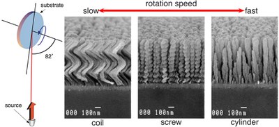
Figure 1: Nanomorphology of DOD films.
Designing Deposition Processes Using Original Growth Simulator
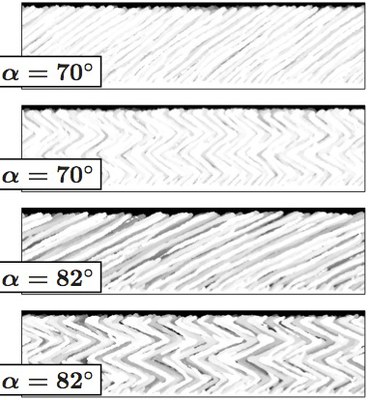
Figure 2: Morphology of simulated films.
Applications of Nanomorphology
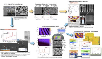
Figure 3: Applications of nanostructured thin films.
Development of Novel Growth Techniques
Nanowire Growth by High Temperature Glancing Angle Deposition
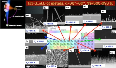
Figure 4: Metal nanowires grown by HT-GLAD.
