Nanomaterials Engineering
The recent nanotechnology focuses on the 'mesoscopic' systems ranging from 1 nm to 1 µm. Their size is medium between that of the microscopic system such as atoms and molecules (0.1 nm) and that of macroscopic system found in our life space (> 1 cm). The mesoscopic systems often show peculiar properties physically and chemically different both from microscopic and macroscopic systems.
We investigate the interaction of ion beams with solid surfaces, and its application to the structural analysis in the mesoscopic region. We are also engaged in developing new techniques of ion-beam processing and ion-beam analysis.
Academic Staff
* Add ".kyoto-u.ac.jp" to each E-mail address.
Kaoru NAKAJIMA
 Associate Professor (Graduate School of Engineering)
Research Interests
He studies ion-solid interactions from various phenomena during collisions between energetic ions and solid target. He also works on improvement of high-resolution Rutherford backscattering spectroscopy (HRBS) and development of new materials using HRBS.
Contacts
Room b4S02, Building C3, Katsura Campus
TEL: +81-75-383-3707
E-mail: kaoru@kues
Research Topics
Studies on interactions of fast ions with solid surfaces
Ion beams produced by accelerators are utilized in various techniques related to the nanotechnology such as surface analysis, surface modification, synthesis of new materials, ion beam micromachining. Understanding of the interaction of fast ions with solids especially with surfaces is a key issue to develop those techniques.
When fast ions are incident onto a solid surface at a glancing angle, they do not penetrate into the solid but just into the region very close to its surface before being reflected specularly. This phenomenon called specular reflection of fast ions is very suitable to investigate ion-surface interactions.
Figure 1 shows what happens during the specular reflection of fast ions. Backscattering of ions, sputtering of target atoms, charge exchange between ions and surfaces, secondary electron emission, nuclear reactions may occur. Various kinds of ion beam techniques base on these phenomena.

Figure 1: Schematic drawing of the specular reflection of fast ions at a solid surface.
Development of high-resolution RBS and downsizing of its system
Atomic-scale analysis technique with higher resolution of sub-nm is needed for progress of nanotechnology.
We have successfully improved depth resolution of Rutherford backscattering spectroscopy (RBS) from 10 nm to 0.2 nm and pioneered layer-by-layer analysis using high-resolution RBS (HRBS). Figure 2 shows a HRBS spectrum of PbSe(111), in which separate peaks corresponding to Pb and Se atoms in the successive atomic layers is observed.
Commercial HRBS system has been developed jointly with Kobe Steel, Ltd. and it is used in various fields such as development of magnetic thin films and ULSI.
We apply HRBS for development of new materials hand-in-hand with companies and universities at home and abroad. Study for further downsizing and improvement of HRBS system is carried on for wider applications of HRBS, for example, application to in-line check at a factory.

Figure 2: HRBS spectrum of PbSe(111)
Studies on the interaction of cluster ions with materials and its application
An ion consisting of a number of atoms is called a cluster ion. When a material is irradiated with energetic cluster ions, a dense energy deposition occurs in a narrow region around each irradiation position. That is why they can produce anomalous effects that are quite different from those by monoatomic ions. Bombardment with a C60 ion of kinetic energy in MeV range, for example, causes emission of thousands of secondary particles (atoms) from an insulator target such as silicon nitride. We are engaged in elucidate the interaction between energetic cluster ions and various materials, and also developing novel techniques of efficient processing and sensitive surface analysis based on the interaction.
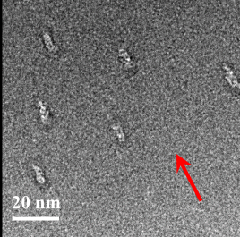
Figure 3 shows a transmission electron micrograph of an amorphous silicon nitride membrane irradiated with 720 keV C60 ions. Cylindrical regions with reduced atomic density (ion tracks) are observed along the paths of every C60 ion.

Figure 3: Transmission electron micrograph of a-SiN membrane irradiated with 720 keV C60 ions.
